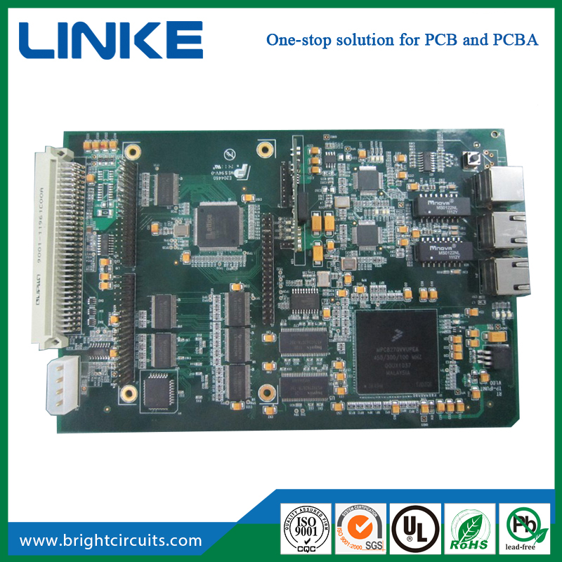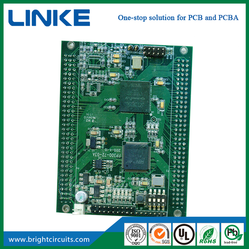
Wave soldering is a batch soldering process used to manufacture jet PCB Assembly, mainly for the soldering of through-hole components. So, what are the issues that need to be paid attention to in the wave soldering process of jet PCB Assembly?

1. There is green oil in the through hole, resulting in poor tin plating in the hole. The green oil in the through hole should not exceed 10% of the hole wall, and the number of holes with green oil should not exceed 5%.
2. The thickness of the coating is not enough, resulting in poor tin plating in the through hole.
3. The thickness of the coating on the through hole wall is not enough, resulting in poor tin plating in the hole. Generally, the thickness of the hole wall should be greater than 18 μm.
4. The hole wall is too rough, resulting in poor tin plating or false soldering in the hole.
5. The hole is wet, causing false soldering or air bubbles. Packaging the PCB when it is not dry or cool, and leaving it for a long time after unpacking, etc., can cause moisture in the holes.
6. The size of the pad is too small, resulting in poor soldering.
7. The inside of the hole is dirty, resulting in poor soldering.
8. Because the hole size is too small, the parts cannot be inserted into the holes, resulting in soldering failure.
9. Due to the offset of the positioning hole, the component cannot be inserted into the hole, resulting in soldering failure.
Shijiazhuang Linke Electronics Tech Co.,Ltd, specializes in prototype pcb assembly, providing electronic OEM processing, DIP plug-in processing, PCBA contracting, PCB circuit board manufacturing and other services, with advanced production equipment and perfect after-sales service system.
Leave a Reply